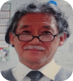
ICCCAS 2024 Invited Speaker
 Yoshiaki Daimon Hagiwara (FIEEE)
Sojo University, Japan
Biography: Hagiwara
graduated California Institute of technology (Caltech) in Pasadena,
California in USA with BS71 with honor, MS1972 and PhD1975 with the major in
Electric Engineering and with the minor in Physics. In February1975, he
joined Sony in Tokyo, Japan and was engaged first in the early development
of Sony image sensors. While working for Sony from 1975 to 2008, he was
engaged in the early developments of image sensor and the digital camera
chip set including the ADC, DRAM and high-speed Cache SRAM buffer memory
chips and micro controller chips. Before retiring from Sony at the end of
July 2008, he was engaged in the PS2 and PS3 chip set developments. He was
invited to talk at CCD1979, ECS1980, ESSCIRC2001, ESSCIRC2008 and ISSCC2013.
While working at Sony until July 2008, he was serving as a visiting
professor at Caltech since 1998 to 1999 in the office of Prof. C. A. Mead in
Electrical Engineering department and also in the offices of Prof. T.C.
McGill and Prof. James McCaldin in Applied Physics department. He was also
serving as a visiting professor since 2003 till 2006 in the office of Prof.
Haruo Kobayashi in Electrical Engineering department at Gunma University in
Japan.
In 1992 he also served as a member of JEDEC memory standardization committee
and also as the IEC TC47 technical committee chair of the international
standard committee (IEC). He also served as the international program chair
and an operational committee member in IEEE EDS sponsored ICMTS conferences,
IEEE ISSCC conferences for which he served as the ISSCC Asian Committee
chair and also as the ISSCC international technical program committee (ITC)
chair in series. He was also a member in the program committee (PC) and the
operational committee (OC) and is now serving in the advisory committee (AC)
of the IEEE Cool Chips conferences in series. He also taught from 2020 to
2021 the AIPS, Artificial Intelligent Partner System for AI robotics at
Kanagawa Institute of Technology in Japan.
In 2008 he founded and worked as the president of Artificial Intelligent
Partner System, AIPS, a nonprofit research organization, NPO, registered by
Kanagawa prefecture government in Japan. Since 2017, he is serving as an
operational committee (OC) member and also as a technical program committee
(PC) member of Department of Education in Society of Semiconductor Industry
Specialists (SSIS) in Japan. Since 2009 till 2017, he taught graduate and
undergraduate students as a full professor of Information and Communication
Science department and is still now serving as a specially appointed
professor at the president office in Sojo University in Kumamoto-city, Japan
working for developments of semiconductor chips for AIPS robotics and Solar
Cell energy solutions. He is Caltech Distinguished Alumni, IEEE Life Fellow
and AAIA Fellow.
Speech Title: Review of Historical Development Efforts of
Solid-State Image Sensors and Solar Cells
Abstract:
This paper reviews historical development efforts of solid-state
image sensors and solar cells and discusses the advantage of the
double-junction type photodiode used in image sensors over the single
junction type photodiode which is still now being used widely in solar cell
applications.
In early 1960s, a solid-state image sensor was typically composed of a
floating-surface N+P single junction type photodiode and a 1T1C DRAM type
read-out circuit with the large output data-line capacitance, causing the
serious CKT thermal noise and the TV scanning clocking-noise. Peter Noble
invented in 1968 the active-pixel image sensor which was a combination of
the in-pixel source-follower type current-amplifier circuit. In 1969, Boyle
and Smith invented a MOS version of a capacitor, which would confine an
electric charge in a nonconductive oxide layer between two parallel metal
layers. In the same year 1969, Michael F. Tompsett invented imaging
charge-coupled devices (CCDs) and in the next six years grew the technology
from eight-bit chips to 512 x 512 element arrays that matched
television-screen resolution in the 1970s.
The surface-channel type CCD had a poor charge transfer efficiency because
it makes use of the silicon surface inversion region which has many charge
trapping centers. On the other hand, the buried-channel type CCD makes use
of a completely-depleted buried signal-charge storage and transfer region,
isolated and freed from the surface charge trapping-centers, resulting in an
excellent charge transfer efficiency of more than 99.999%. The final stage
of the CCD operation is characterized by charge-transfer induced by the
relatively large fringing electric fields induced in the buried charge
storage depletion region, where majority-carrier electrons can be depleted
and completely drained. The residual charge decays exponentially, draining
even a single photo electron charge in the high-performance and
high-frequency buried channel CCD devices.
In solar cell applications, on the other hand, both the high frequency
operation of CCD devices and the in-pix active source-follower amplifier
circuits are no longer needed. However, the transfer efficiency of a single
photo electron charge, generated in the sun-light lit photodiode to the
output terminal, is very important in order to achieve a high quantum
efficiency in solar cell applications. This paper explains and concludes
that the completely majority-carrier depleted buried photo charge storage
and transfer region in the PNP double junction Pinned Photodiode type Solar
Cell is the answer to achieve a high quantum efficiency of solar cells.
